IBM 和 Cadence:利用复杂的 PCB 系统简化大型计算机设计

技术
- 处理器与边缘智能 - 微控制器与印刷电路板 (PCB)
- 传感器 - 温度传感器
适用功能
- 产品研发
用例
- 制造过程模拟
- 时间敏感网络
服务
- 硬件设计与工程服务
- 系统集成
关于客户
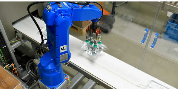
50 多年来,IBM 一直是大型机计算领域的领先企业。该公司以其大规模设计而闻名,制造出采用高度复杂印刷电路板 (PCB) 的大型计算机。这些 PCB 是超小型元件的巨大配置,单板在 10 多层电路中承载数万个信号互连。这些设计非常复杂,每个组件的引脚数达到 5,000 个,板级连接数超过 5,000 个,带来了重大的设计挑战。尽管面临这些挑战,IBM 仍在继续创新并在大型机计算领域处于领先地位。

挑战
IBM 是大型机计算领域的领导者,在为其大型计算机设计高度复杂的印刷电路板 (PCB) 时面临着挑战。这些 PCB 尺寸高达 50 厘米 x 60 厘米,在 10 多层电路中承载数万个信号互连,每个组件的引脚数达到 5,000 个,板级连接数超过 5,000 个。这些设计的复杂性使得传统原理图的处理和分析变得麻烦且耗时。 IBM 试图通过开发一种解决方案来简化该流程,该解决方案以表格或电子表格格式输入每个信号的设计属性。然而,这又增加了一个步骤,因为工程师必须将信息转换为硬件描述语言 (HDL) 才能与设计平台交互。此外,模拟元件不能以这种方式处理,必须手动配置。
解决方案
IBM 德国研发实验室采用了 Cadence 的 Allegro System Architect GXL,这是一种集成解决方案,可在完整的设计和仿真环境中管理表格和原理图数据。该解决方案使设计人员能够像使用会计电子表格一样轻松地输入和操作信号规格,将输入时间减少到直接处理原理图所需时间的十分之一,并且错误更少。该解决方案还实现了快速编译,将设计代码编译时间从 8-10 小时缩短到几秒钟。这样可以快速检测错误并提高效率和生产率。 Allegro System Architect GXL 的集成环境还允许工程师更快、更轻松地评估前端定义将如何影响后端设计问题,从而将 PCB 开发所需的时间减少 80%。
运营影响
数量效益

Case Study missing?
Start adding your own!
Register with your work email and create a new case study profile for your business.
相关案例.
Case Study
Battery manufacturer Industrial Digital Twin
For optimum control of product quality, Banner relies on a high production depth. Its 560 production employees produce nearly all the components in¬-house that they need to make finished batteries on Banner’s six assembly lines. This includes the plastic parts for the battery cases as well as the paste-filled lead oxide grids. Their production involves two to five¬ days rest in maturing chambers to create optimum current absorption and storage capacity. Banner’s ongoing success was accompanied by a continuous, organic growth of the production facilities, adding or extending hall after hall until the complex filled the site that had seemed ever so spacious when the company moved here from a smaller place in 1959. These developments led to a heterogeneous production environment. “This confronts us with significant challenges, particularly concerning intra¬logistics issues, such as scheduling for the maturing chambers,” says Franz Dorninger, technical director at Banner. “We contemplated various ways to overcome this problem, including relocating to new premises.”
Case Study
Centralizing Data for Improved Efficiency: A Case Study on Malvern Panalytical
Malvern Panalytical, a UK-based hi-tech electronics company, was grappling with the challenge of decentralized data storage. The company had a vast amount of unstructured data scattered across various platforms, from hard drives to emails and floppy disks. This made the data searching process extremely cumbersome and inefficient. The company's rapid growth, from 200 to over 1,000 employees in a decade, and expansion across three continents further exacerbated the need for a more structured and centralized data system. As a company involved in electronics manufacturing and software development, it was crucial for Malvern Panalytical to find a platform that could structure all their data, track all modifications of documents in real time, and provide clear visibility of the internal information flow across all its facilities.
Case Study
Managed Hosting Platform
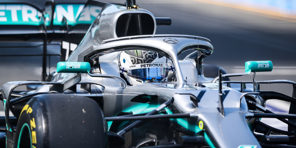
Formula 1® is a sport where every millisecond matters. With changing preferences and the growth of the digital medium, many fans choose to experience the sport through the F1.com website. The website needs to deliver a superior experience to tens of millions of fans across the world consistently. Hence, it is imperative to have a robust platform that can deliver the required performance and scale with growing trac and dynamic fan expectations. Some of the key challenges are: • Every race weekend, Formula1.com attracts up to 7 million fans. Managing this huge surge in website traffic, requires a scalable hosting platform that can simultaneously allow millions of fans to experience the excitement of the sport seamlessly. • Fans across the globe expect an engaging and immersive experience through enriched and enhanced race content across multiple devices. To meet this requirement Formula1.com needs to have a robust platform that is able to deliver real-time updates and information across screens, be it tablets, TVs or smartphones. • A global brand like Formula 1® needs to ensure it delivers a consistent user experience across all platforms across the globe. This consistent delivery of enriched content cannot be compromised through downtime or any other issue at any point. • In an age where threats to global websites are prevalent, Formula 1® needed a platform that was ready to meet any challenge to its website. They needed a solution that delivers consistency, scalability and yet at the same time is continuously monitored, secure and reliable.
Case Study
Flow Robotics: Scaling Up Production and Accelerating Product Development with IoT
Flow Robotics, a Danish manufacturer, developed flowbot™ ONE pipetting robots to alleviate the strain on bioanalysts in life-science laboratories and hospitals across Europe. These robots were designed to automate part of the testing process, speeding up the time it takes to produce results and reducing pressure on staff. However, the company faced challenges in scaling up production and accelerating product development. High workloads and physically challenging conditions have long been an issue for laboratory professionals. Flow Robotics estimates that around half of medical lab technicians carry out the same arm movements for at least a quarter of their working day. The American Society for Clinical Pathology reported that 85% of laboratory professionals feel burnt out; 36% struggle with inadequate staffing; and 32% face a heavy workload and pressure to complete all testing on time.

Case Study
EDF's Transformation: Enhancing Employee Experience through IT Modernization
EDF, a major UK utilities company, was grappling with a highly customized service management system that was largely manual, with limited potential for automation. This made it difficult to predict or prevent system failures and provide a resilient service. The company's IT system for incident handling was purely manual, leaving no room for modernization. EDF wanted to serve its business and residential customers better by improving the response time to rising energy demands. To achieve this, the company needed to provide its employees with the right tools for improved productivity, better collaboration, and an enhanced IT experience at a reduced cost to serve.
